Click to view our Accessibility Statement or contact us with accessibility-related questions


Showing 1 of 74 conversations about:

Pawnerd
220
Pawnerd
Mar 9, 2018
bookmark_border
GrendelFor what would you like to see the schematics?
In case you are wondering and couldn't find more about the headers, here they are from top left to right bottom (chip inside is an atmega32u4):
Miso, Vcc, SCK, Mosi, Reset, Ground
Vcc, UART RX, UART TX, GPIO1/SDA, GPIO2/SCL, Ground
Fuse is placed in the circuit to cut of somewhere between 0.5 to 1.1 ampere.
Fuse is placed in the circuit to cut of somewhere between 0.5 to 1.1 ampere.
Grendel
131
Mar 9, 2018
bookmark_border
PawnerdThat helps for hooking up the ISP :) Altho, "top left" when viewed how ? I prefer to run my own KB firmware whenever I can, need the schematic for porting it.
Pawnerd
220
Pawnerd
Mar 9, 2018
bookmark_border
Grendelwhen you look from the back to the device when yoh can see the pins.
You can find the pin layout of the keyswitches on github.com/qmk/qmk_firmware/keyboards/knops/mini/ (I am not sure if this link is completely correct, currently on mobile)
You can find the pin layout of the keyswitches on github.com/qmk/qmk_firmware/keyboards/knops/mini/ (I am not sure if this link is completely correct, currently on mobile)
Grendel
131
Mar 9, 2018
bookmark_border
PawnerdThanks.
The link is https://github.com/qmk/qmk_firmware/tree/master/keyboards/knops/mini ;) I much prefer reading a schematic over digging the info out of source code, hence my asking. Esp. since it's more than just the switches -- LED's, speaker, HWB (going to replace the bootloader), to name a few of the top of my head.
The link is https://github.com/qmk/qmk_firmware/tree/master/keyboards/knops/mini ;) I much prefer reading a schematic over digging the info out of source code, hence my asking. Esp. since it's more than just the switches -- LED's, speaker, HWB (going to replace the bootloader), to name a few of the top of my head.
Grendel
131
Mar 9, 2018
bookmark_border
PawnerdHm, trying to talk to the chip w/ a JTAGICE mkII in ISP mode fails :(
Edit: got it working after taking it apart and measuring some continuity -- turns out that the sequence "Miso, Vcc, SCK, Mosi, Reset, Ground" is from right to left when looking at the pins. :/
Edit: got it working after taking it apart and measuring some continuity -- turns out that the sequence "Miso, Vcc, SCK, Mosi, Reset, Ground" is from right to left when looking at the pins. :/
Pawnerd
220
Pawnerd
Mar 9, 2018
bookmark_border
PawnerdI will prepare them for you and make them public + share info here. if you don't have an answer by monday, I might have forgotten about it.
Pawnerd
220
Pawnerd
Mar 13, 2018
bookmark_border
GrendelKeyswitches are connected to ground on one side and a digital gpio pin of the atmega32u4 on the other side. The gpio pin of the 32u4 is floating when keyswitches are not pressed and connected to ground once they are being pressed.
Each keyswitch has a led as well. These are connected to a gpio of the 32u4 on one side and ground on the other
The three layerleds are a bit different regarding to keyswitch leds in that the first and third is connected to a gpio pin on one side and Vcc on the other. The second layer led is connected to a gpio pin and ground. This has to do with arduino compatibility, layerled 1 and 3 replace the RX and TX leds you will normally find on the Arduino Leonardo.
The speaker is connected to two pins, so that you can make multiple tones at the same time.
pins per keyswitch: keyswitch 1: PF7 keyswitch 2: PF6 keyswitch 3: PF5 keyswitch 4: PF4 keyswitch 5: PF1 keyswitch 6: PF0
pins per led (for keyswitches): led 1: PD7 led 2: PC7 led 3: PD4 led 4: PE6 led 5: PB4 led 6: PD6
pins per led (for layer indication): led 1: PD5 (to Vcc) led 2: PB6 (to Gnd) led 3: PB0 (to Vcc)
pins for speaker: one side: PC6 other side: PB5
Pawnerd
220
Pawnerd
Mar 14, 2018
bookmark_border
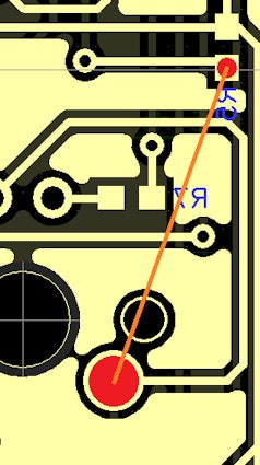
GrendelNo, it's pulled up to 5V with a 10k ohm (R5) resistor.
Pawnerd
220
Pawnerd
Mar 14, 2018
bookmark_border
Grendelare you sure? I believe you would only need that to change the bootloader, not? If so, it won't be very hard to solder a wire between the smd resistor and a pin of one of the switches.
Grendel
131
Mar 14, 2018
bookmark_border
PawnerdYea, need it to have RESET invoke the bootloader. Prefer that over always starting w/ the loader and examining MCUSR.
Pawnerd
220
Pawnerd
Mar 14, 2018
bookmark_border
Grendelthe bootloader that is currently on it checks if the third keyswitch is being pressed. If it is, it goes into DFU mode, if not it goes directly to the application. As long as you can generate a hex file, you can use flip, qmktoolbox or the old kbflasher tool to upload new firmware.
Grendel
131
Mar 14, 2018
bookmark_border
PawnerdBack in the day I wrote a Teensy compatible bootloader that I use in pretty much anything to keep things simple :)
Pawnerd
220
Pawnerd
Mar 15, 2018
bookmark_border
Grendelaah okay, well you can use it since all pins required are open to use (with some extra steps for the hwb pin). Good luck! Let me know if you need any more help (or the old bootloader hex file if you find out you might have messed up just a little bit)
Related Products


Drop Refurbished
Like-new products you can trustDrop Rewards
Get $5 for every 500 points you earn! Learn more
Drop Keyboard Club
Become a member and expand your keycap collectionCollaborate With Us
For Brands & DesignersFollow Drop